
Ahora estás siguiendo a
Error al seguir a usuario.
Este usuario no permite que los usuarios lo sigan.
Ya estás siguiendo a este usuario.
Tu plan de membresía solo permite 0 seguimientos. Mejora tu membresía aquí.
Dejaste de seguir correctamente a
Error al dejar de seguir al usuario.
Has recomendado exitosamente a
Error al recomendar al usuario.
Algo salió mal. Por favor, actualiza la página e intenta de nuevo.
Email verificado correctamente.

ahmedabad,
india
Aquí son las 11:10 p. m.
Se unió el abril 21, 2016
1
Recomendación
Maulik P.
@maulik1717
3,6
3,6
100%
100%
ahmedabad,
india
100 %
Trabajos finalizados
11 %
Dentro del presupuesto
11 %
A tiempo
50 %
Tasa de recontratación
Pcb layout in allegro and altium. DFM in genesis
Contacta Maulik P. sobre tu trabajo
Inicia sesión para comentar cualquier detalle por chat.
Portafolio
Portafolio
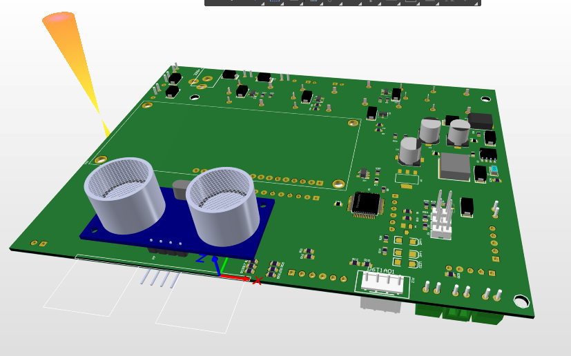

Pcb Layout of Automatic hand sanitizer.

Pcb Layout of Automatic hand sanitizer.
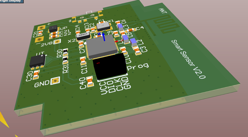

BleTemperaturesensor

BleTemperaturesensor
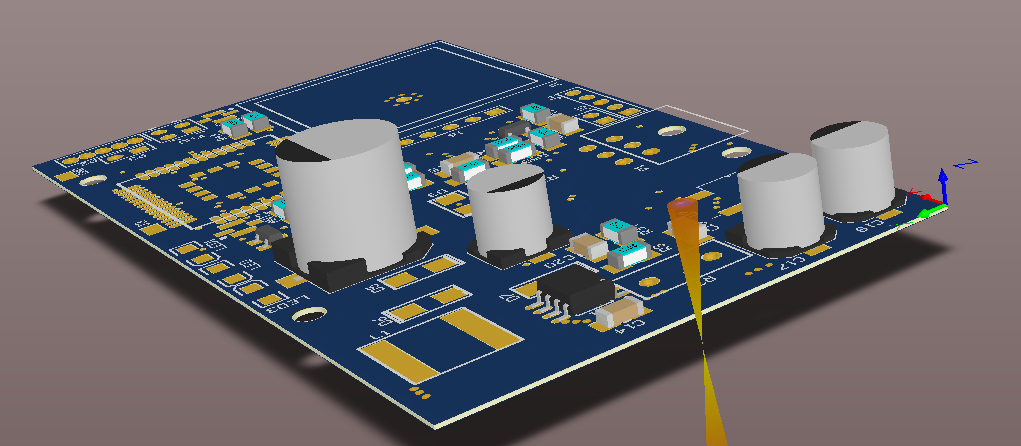

Personal tracking system

Personal tracking system
Pcb Layout of Automatic hand sanitizer.
Pcb Layout of Automatic hand sanitizer.
BleTemperaturesensor
BleTemperaturesensor
Personal tracking system
Personal tracking system
Comentarios
Cambios guardados
Mostrando 1 - 2 de 2 reseñas
$217,49 USD
PCB Layout
T
•
$27,00 USD
Electronics
Microcontroller
Electrical Engineering
PCB Layout
Circuit Design
T
•
Experiencia
design single side, double sided and multilayered PCBs
oct 2006 - Presente
1. Worked on design single side, double sided and multilayered PCBs using industry standard techniques.
2. Generate and maintain Gerber and CAM.
3. CAD library administration including symbol, footprint generation and database administration.
4. BOM preparation.
5. Gerber / ODB++ files(Fabrication/Assembly files) Validate by using Valor Genesis 2000 & CAM350
Educación
B.E In EC
(4 años)
Contacta Maulik P. sobre tu trabajo
Inicia sesión para comentar cualquier detalle por chat.
Verificaciones
Principales habilidades
Explorar freelancers similares
Explorar galerías similares
¡Invitación enviada correctamente!
¡Gracias! Te hemos enviado un enlace para reclamar tu crédito gratuito.
Algo salió mal al enviar tu correo electrónico. Por favor, intenta de nuevo.
Falló el copiado al portapapeles. Intenta de nuevo después de ajustar tus permisos.
Copiado al portapapeles.
Cargando visualización previa
Permiso concedido para Geolocalización.
Tu sesión de acceso ha expirado y has sido desconectado. Por favor, inica sesión nuevamente.